Tandem racing: how scientists build the perfect solar cell (I/II)

· 10 min read
This is part one of a two-part series on energy storage technologies. You can find part two here.
In a groundbreaking revelation during the summer of 2023, Stefaan de Wolf's team introduced a solar cell achieving a record 33.7% efficiency, eclipsing the performance of leading commercial products by nearly 10%. This surge in efficiency is credited to the innovative two-layer silicon-perovskite tandem design, which surpasses conventional single-layer cells. This article delves into the science behind these high-efficiency cells, investigating how they efficiently convert sunlight into electricity and the materials and technologies enabling this achievement.
On the first day of summer 2023, Stefaan de Wolf’s group announced that they had created a solar cell with a record efficiency of 33.7 percent. This surpasses the best commercial products by almost ten percent. The trick here is that all the latest record-breaking elements are two-layer. We will tell you why silicon-perovskite tandems began to overtake their single predecessors, how they look like Formula 1 cars and who is the favorite in this race.
The main metric distinguishing a good solar cell from a worse one is its efficiency (or COP). This value shows how much of the total energy of sunlight that fell on the surface of the battery was converted into electricity.
This transformation is a multi-stage process, and energy losses occur at each stage: from the absorption of light to the transfer of electrons directly into the electrical circuit. Therefore, the overall efficiency of the element is usually lower, depending on the number of defects in the semiconductor, the quality of the contacts, the thickness of the active layer, and design features.
But there is one fundamental limitation here — the band gap of the semiconductor on which the solar cell operates. It determines how much sunlight an element can, in principle, absorb and how many electrons capable of conducting current will appear in its active layer.
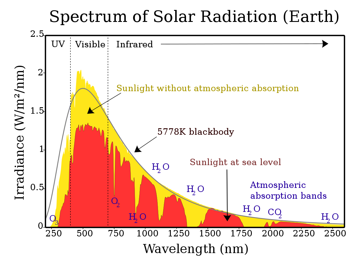
The spectrum of solar radiation: the wavelength is plotted along the horizontal axis (it is inversely proportional to the photon energy), the spectrum is shown in yellow light without the influence of atmospheric absorption, in red — reaching the earth’s surface.
For a solar cell to work efficiently, as many photons as possible must convert the non-conducting electrons in the semiconductor to conductive ones. To this end, you need to choose a material in which the forbidden zone will be of a suitable size.
If the bandgap is too wide, most of the photons will pass through the solar cell and not be absorbed. The effectiveness of such an element, of course, will not be high. But even a material with a too-small band gap will not make the element effective. From one photon all the same, only one pair of electron-hole is obtained, and the rest of the energy is dissipated in the form of heat. In addition, most of the light is absorbed in the near-surface region of the semiconductor, so this region heats up quickly, which can be harmful to the solar cell.
It turns out that with an increase in the band gap, the fraction of useful solar energy first increases and then begins to decrease. For the kind of light that falls on the surface of our planet (most of the photons in it have an energy of about 2.5 electron volts), the maximum of this curve (that is, the optimal value of the band gap) is around 1.34 electron volts.
However, even if a material with a band gap of precisely this width can be discovered and used to construct a solar cell, its efficiency will still not reach one hundred percent. In 1961, Nobel laureates William Shockley and Hans-Joachim Queisser calculated that taking into account all losses, the efficiency of a single-layer solar cell could in principle not be higher than 30 percent. The Shockley-Queisser limit has been refined several times, and today the generally accepted limit value is 33.7 percent.
This means that even in an ideal scenario, little more than a third of solar energy can be converted into electricity. The rest is lost: 47 percent of the energy will turn into heat, 18 percent will not be absorbed at all, and another 0.2 percent will be lost due to the recombination of newly generated electrons and holes.
Silicon turned out to be one of the closest to the ideal — it has a band gap of between 1.12 and 1.15 electron volts. This is slightly less than the optimal 1.34 electron volts, so the theoretical maximum will be below the Shockley-Queisser limit: about 29.4 percent.
By and largy, humanity has been remarkablylucky with silicon. Not only does it possess a band gap of the required width, but it is also quite inert. In addition, silicon and its compounds are often found in the earth’s crust. Therefore, silicon solar cells are easy to produce, stable, and well-studied. The efficiency record that has been achieved so far for silicon is 26.1 percent, only three percent below the theoretical maximum. And the best cells, which are mass-produced, have already reached 24 percent.
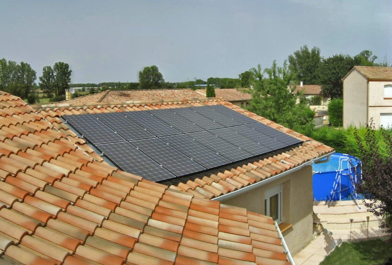
Silicon solar cell on the roof of a house in Italy. David TREBOSC / flickr
True, high efficiency comes at a cost. Silicon for solar cells must be very pure — at least 99.9999 percent (one impurity atom is allowed for every million silicon atoms). To obtain such crystals, silicon is heated to temperatures above one and a half thousand degrees Celsius, this is a very long and expensive process.
As technology improves and large-scale production opens in China and the United States, silicon cells, and with them solar electricity, are gradually becoming cheaper: in 2020, the cost of a kilowatt-hour in some regions dropped to 0.04 US dollars. But technology cannot be improved indefinitely, and pretty soon solar cells will cease getting cheaper. To rival silicon cells, a significantly cheaper or markedly more efficient alternative is necessary. And ideally, of course, — both would be preferable. However, potential competitors remain distant.
For example, gallium arsenide GaAs (and other compounds from group III-V) have a band gap closer to the optimal value than silicon, and elements based on it have already reached an efficiency of 29.1 percent. But such batteries are noticeably more expensive than silicon ones, and besides, the stocks of raw materials for them are limited. Organic solar cells, on the contrary, are cheaper, but inefficient (less than 20 percent), and most importantly, not very stable. The main competitor now is solar cells based on perovskites, mixed lead halides with the general formula APbI3. They are also cheap and in ten years have caught up with silicon in efficiency. Now the record for these species is the same — 26.1 percent.
With the term “perovskite” in modern scientific literature, everything is not easy. Initially, perovskite is the mineral CaTiO3 (calcium titanate), which was discovered in the Urals in 1839. The name was given in honor of the Russian minister Lev Perovsky, who was interested in mineralogy. CaTiO3 has a very characteristic crystal lattice: titanium cations are located at the vertices of the cubic cell, larger calcium cations are located in the center of the cell, and oxygen anions are located on the edges of the cube, forming TiO6 octahedra around each titanium ion, connected by common vertices. This crystal lattice was called the perovskite lattice. Gradually, other compounds with the formula ABX3 and such a structure of the crystal lattice began to be called perovskites in the literature.
Perovskites, which are used in solar cells and other semiconductor devices, are very far from CaTiO3 in terms of chemistry. Instead of oxygen, they contain iodine, instead of titanium—lead, and instead of calcium cesium or organic cations of methylammonium and formamidinium. Even the charge of each ion is only half that. However, the APbI3 crystal lattice has the same structure as the CaTiO3 lattice: PbI6 octahedra are located at the lattice sites, and larger organic or cesium cations are located in the voids between them.
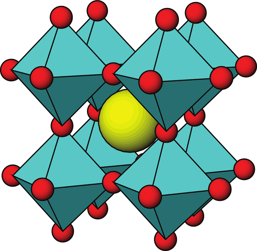
The structure of the crystal lattice of perovskite. Halogens are shown in red, large cations of type A are shown in yellow; lead cations are inside turquoise octahedrons. Priyanka Roy et al. / Coatings, 2023
However, perovskite elements still have serious problems with stability. In addition, they also approach the theoretical efficiency ceiling — new records appear less and less. And even if an efficiency of 30 percent on perovskites is in principle achievable, it will take a long time to get to it.
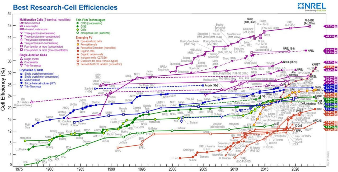
Efficiency records by the US National Renewable Energy Laboratory (NREL) for different types of solar cells. NREL
Since there is no direct replacement for silicon, and more efficient and cheaper elements are still needed, the scientists proposed adding something to it that would inexpensively expand the range of absorbed light. For example, an additional layer of the second semiconductor.
In such tandem elements, the upper translucent layer is made of a semiconductor with a wide band gap, it absorbs only the highest energy photons. Photons with lower energy pass into the lower layer with a narrower band gap and are absorbed already there. Thus, you can kill two birds with one stone: absorb a large proportion of solar radiation, and prevent the element from heating up too much.
Silicon has a band gap of less than the optimal 1.34 electron volts, so it’s a great fit for the bottom of the tandem. For a semiconductor for the upper layer of such a tandem, the band gap (both according to theoretical calculations and according to experimental comparison data) should be about 1.7 electron volts — in this case, each photon will be absorbed where it can make the greatest contribution to efficiency.
Perovskites turned out to be the best candidate for partners with silicon. Solar cells are made from them by “wet chemistry” methods in mild conditions. Therefore, the perovskite layer can be applied over an already-finished silicon element. By changing the composition of perovskite (for example, replacing part of the iodine in its lattice with bromine and chlorine), one can choose the desired value of the band gap with an accuracy of a hundredth of an electronvolt.
The first silicon-perovskite solar cells appeared in 2015. These were four-terminal tandems — with a separate pair of contacts for each semiconductor layer. Such a tandem consisted of two separate solar cells, made separately and fastened only mechanically. At the same time, the authors tried to make all the layers in the outer perovskite element, through which the light passed first, as transparent as possible (of course, except for the directly active perovskite layer), so that not a single photon was absorbed in vain.
True, the results of the first experiments turned out to be disappointing — the efficiency was only 13.4 percent, which at that time was already even lower than that of each of the parts separately.
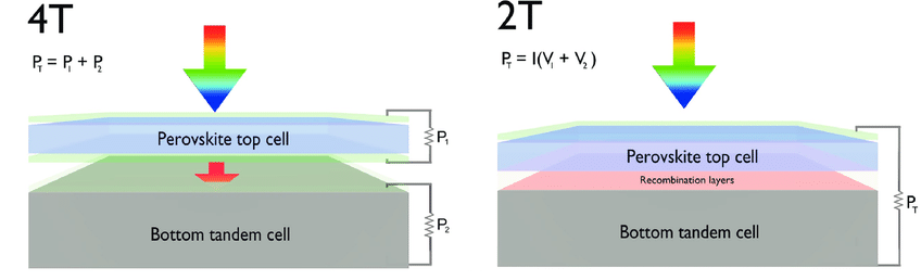
The structure of a tandem solar cell in a four-terminal (left) and two-terminal (right) configuration. In a two-terminal configuration, there is a recombination layer between the silicon and perovskite layers. Lai et al. / Advanced Energy Materials, 2017
Therefore, in parallel with four-terminal tandems, scientists have begun to work on an alternative scheme — a two-terminal cell. In such elements, two semiconductors are connected not only mechanically, but also electrically. The element has only one pair of contacts: electrons go from one semiconductor to the circuit, and holes from the other. The connection is in series so that the voltage produced by the two cells is summed. For better performance, they try to equalize the current in two parts — usually this is achieved by changing the thickness of the perovskite layer.
Making two-terminal tandems, on the one hand, is easier: they have fewer layers. On the other hand, it is more difficult: perovskite has to be applied directly on top of the silicon element. However, the requirements for maximum transparency of all auxiliary layers remain the same as for the four-terminal tandem.
The most popular are two-terminal tandems, in which electrons are removed from the perovskite part, and holes from the silicon part. For electron transport, thin layers of fullerenes and their derivatives are used in them, and to facilitate the extraction of electrons, magnesium fluoride or lithium fluoride is applied between perovskite and fullerene.
Improved silicon-perovskite tandems have dramatically overtaken: already in 2018 they bypassed silicon, at the end of 2020 they overcame the theoretical limit for silicon, and in 2022 they were the first among solar cells to reach a height of 30 percent efficiency.
Illuminem Voices is a democratic space presenting the thoughts and opinions of leading Sustainability & Energy writers, their opinions do not necessarily represent those of illuminem.
illuminem briefings

Oil & Gas · Energy Sources
illuminem briefings

Coal · Public Governance
illuminem briefings

AI · Power Grid
The Guardian

Coal · Ethical Governance
Financial Times

Minerals · Energy Sources
CBC

Battery · Energy Sources